
TL;DR:
- The optical chip security market focuses on protecting photonic circuits from physical and signal-based threats using unique techniques like Layer 1 encryption and quantum key distribution. As threats posed by optical eavesdropping and light emission side-channels grow, organizations must adopt specialized hardware, monitoring, and quantum-safe solutions. Future growth emphasizes photonic PUCs, quantum-resistant cryptography, and architecture shifts like 3D integration, demanding organizations treat photonic security as a distinct domain requiring tailored strategies.
The optical chip security market sits at the intersection of photonics, cryptography, and hardware defense. Most security professionals still think of chip-level threats in terms of electronic vulnerabilities, but photonic systems introduce an entirely different attack surface, one where light itself becomes the vector. What is the optical chip security market? It is the rapidly expanding segment of the security industry dedicated to protecting photonic and optical integrated circuits from physical interception, signal manipulation, and unauthorized access. With quantum computing timelines compressing and AI driving unprecedented optical bandwidth demand, understanding this market is no longer optional for anyone operating at the edge of secure infrastructure.
Table of Contents
Key Takeaways
| Point | Details |
|---|---|
| Market size and growth | The global optical encryption market is projected to reach $7.96 billion by 2031, growing at an 8.62% CAGR. |
| Photonic attack vectors are distinct | Optical chips face unique threats including optical eavesdropping and light emission side-channels not present in electronic chips. |
| Layer 1 encryption dominates | Hardware-based Layer 1 encryption held 45.60% market share in 2025 and is the preferred solution under zero-trust mandates. |
| Photonic PUCs are accelerating | The photonic physical unclonable chip market is growing at a 22.4% CAGR, reaching a projected $9.5 billion by 2033. |
| Quantum-secure methods are becoming standard | Quantum key distribution and quantum random number generation are transitioning from research to deployed infrastructure. |
Optical chip security market overview and growth
The global optical encryption market was valued at $4.85 billion in 2025 and is projected to reach $7.96 billion by 2031 at a CAGR of 8.62%. That trajectory reflects more than general security spending growth. It reflects a structural shift: organizations moving from software-layer protections toward hardware-embedded optical encryption because software-layer defenses cannot address physical-layer optical threats.
The market segments across three primary categories.
-
Hardware encompasses optical encryption appliances, photonic integrated circuits, and dedicated optical security modules deployed directly in transmission infrastructure.
-
Software covers management platforms, key management systems, and anomaly detection tools that operate alongside optical hardware.
-
Services include deployment, integration, and monitoring support, which is growing particularly fast as enterprises lack in-house photonic security expertise.
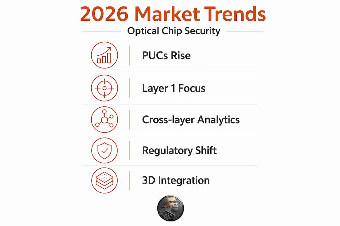
The fastest-growing subsegment is the photonic physical unclonable chip (PUC). These devices exploit the inherent randomness of light scattering within their physical structure to generate unique, unclonable hardware identifiers. The photonic PUC market was valued at $1.28 billion in 2024 and is projected to reach $9.5 billion by 2033 at a 22.4% CAGR. That growth rate is significantly higher than the broader optical encryption market, signaling that device authentication and anti-counterfeiting applications are outpacing general encryption deployment.
Applications fueling the overall market include data-center interconnect encryption, telecom backbone security, IoT device authentication, and government-grade secure communications. North America currently leads in market share, driven by defense procurement and hyperscale data center density, while Asia-Pacific is the fastest-growing region due to expanding 5G infrastructure and national quantum communication programs.

Pro Tip: When evaluating optical encryption vendors, ask specifically which OSI layer their solution encrypts at. Layer 1 solutions encrypt the optical signal before framing, which means they protect data regardless of the protocol stack above. Many vendors conflate Layer 2 and Layer 1 when positioning their products.
How optical chip technology creates unique security challenges
Understanding what is optical chip technology requires separating it from conventional semiconductor assumptions. Electronic chips process data using electrons. Photonic chips process it using photons, which means signals travel at the speed of light, generate minimal heat, and offer substantially higher bandwidth density. Those same properties create attack vectors with no analog in electronic security.
Photonic chips face unique threats including optical signal interception and light emission side-channels that electronic chips do not exhibit. Specific threat categories include:
-
Optical eavesdropping: An attacker can tap a fiber link or waveguide and siphon off a fraction of the optical signal without breaking physical continuity. Unlike cutting a wire, optical tapping leaves the primary signal largely intact, making detection difficult without dedicated monitoring equipment.
-
Side-channel attacks via light emission: Photonic circuits emit detectable optical signatures during operation. Analyzing those emissions can expose timing information, key material, or processing states.
-
Physical tampering and injection: Introducing a rogue optical signal into a waveguide can corrupt data streams or probe circuit behavior in ways analogous to fault injection attacks on electronic chips but executed entirely through light.
-
Supply chain compromise: Photonic components manufactured in untrusted facilities can contain deliberate structural modifications that are invisible to standard electrical testing.
Femtosecond laser writing is one manufacturing technique that addresses some of these concerns at the fabrication level. This process inscribes 3D photonic circuits directly inside borosilicate glass, creating structures with stable, low-loss characteristics superior to silicon photonics for quantum cryptographic applications and long-term durability. Glass-based photonic chips are harder to reverse-engineer and more resistant to certain categories of physical probing.
Effective photonic security requires cross-layer monitoring that integrates optical signal analytics with electronic control-plane security, using sensors and incident response procedures built specifically for photonic systems. This is not a domain where repurposing existing electronic security tooling is sufficient.
Security techniques protecting optical systems
The optical chip security market has produced a distinct set of protective mechanisms, many of which have no direct counterpart in electronic security. Understanding how optical chips enhance security at each layer requires moving through the stack methodically.
-
Layer 1 hardware encryption. This is the market’s dominant approach. Layer 1 solutions held 45.60% market share in 2025, growing at an 11.55% CAGR through 2031. By encrypting the optical signal at the physical layer before any framing or protocol handling, Layer 1 solutions remove the software attack surface entirely. Keys remain in hardware and never traverse a software stack.
-
Physical-layer security mechanisms. Techniques like spectrum randomization, optical coding, and optical spread-spectrum transmission make it significantly harder for a passive eavesdropper to extract meaningful data from an intercepted signal. These methods complement encryption rather than replace it.
-
Quantum key distribution (QKD). QKD is transitioning from theoretical to deployed infrastructure in telecom and government sectors. QKD leverages quantum mechanical properties to distribute cryptographic keys in a way that makes interception physically detectable. Any attempt to observe the key exchange disturbs the quantum state, alerting both parties.
-
Quantum random number generation (QRNG). Researchers achieved a record 42.7 Gbit/s secure random bit generation rate using a quantum coherent receiver chip written into borosilicate glass. High-rate QRNG is critical because conventional pseudo-random number generators are mathematically predictable, which undermines key strength in high-throughput optical systems.
-
Optical monitoring and incident response. Deploying optical time-domain reflectometers and in-band optical power monitors allows operators to detect anomalous signal behavior indicative of tapping or injection attempts. This monitoring layer must be integrated with security information and event management (SIEM) systems configured to handle photonic-specific event signatures.
Pro Tip: QKD and QRNG are not interchangeable. QKD secures key exchange over a channel. QRNG produces unpredictable key material at the source. A genuinely quantum-secure optical system needs both, and vendors that advertise one without the other are offering an incomplete solution.
For teams researching optical encryption methods, the distinction between physical-layer and cryptographic-layer protections is where most security architecture decisions get made incorrectly.
Network architecture and regulatory drivers
The optical chip security market does not exist in isolation from broader infrastructure trends. Two forces in particular are reshaping security requirements faster than most vendors anticipated.
The rise of software-defined elastic optical networks dramatically expands the attack surface. When optical network behavior is programmable via software control planes, compromising the control plane can allow an attacker to redirect traffic, suppress alarms, or manipulate spectrum assignments without ever touching physical fiber. This demands AI-driven anomaly detection and hybrid quantum-secure frameworks that treat the control plane as an adversarial environment rather than a trusted one.
Regulatory pressure is equally significant. Key forces driving hardware encryption adoption include:
-
Zero-trust mandates requiring that encryption keys never be accessible to the operating system or hypervisor layer, which only Layer 1 hardware solutions satisfy.
-
Sovereign cloud regulations in the EU, India, and Southeast Asia that require organizations to maintain physical control over in-flight encryption keys, making foreign-manufactured optical security hardware a compliance liability.
-
Supply chain scrutiny targeting photonic component sourcing, particularly for components manufactured in regions subject to export controls or geopolitical risk.
-
Emerging standards activity from bodies including NIST, ITU-T, and ETSI that are beginning to formalize quantum-safe cryptography requirements for optical transport networks.
The intersection of these regulatory forces with the technical capabilities of spatial computing trust infrastructure is where the most consequential optical security investments are being made today.
Applications and future trends
The optical chip security market spans a wider set of sectors than most market analyses acknowledge. The following comparison illustrates current adoption depth against near-term projected growth across key verticals:
| Sector | Current adoption focus | Near-term growth driver |
|---|---|---|
| Telecom | Layer 1 backbone encryption | QKD network deployment |
| Data centers | High-speed interconnect encryption | AI workload optical fabric security |
| IoT | Photonic PUC-based device authentication | Supply chain anti-counterfeiting |
| Healthcare | Secure optical patient data transmission | Regulatory compliance with quantum-safe standards |
| Finance | Low-latency encrypted trading infrastructure | Post-quantum cryptography migration |
| Defense | Classified optical communications | Integrated photonic secure modules |
The IoT row deserves particular attention. Photonic PUCs generate identifiers from the natural randomness of light scattering during manufacturing, which means no two chips produce the same cryptographic signature even when fabricated on the same production line. For IoT environments where device authentication at scale is a persistent challenge, photonic PUCs offer a hardware-rooted authentication mechanism that is physically impossible to clone.
Looking further forward, the market is converging on three architectural directions: 3D photonic integration (stacking photonic and electronic layers for co-packaged security), silicon photonics at wafer scale for cost reduction, and quantum-secure photonic modules that combine QKD, QRNG, and Layer 1 encryption in a single optical security appliance. The importance of optical chips to next-generation secure infrastructure grows with each of these trajectories.
For a detailed analysis of how optical and computing security approaches diverge at the architectural level, the distinctions matter significantly when planning long-horizon security investments.
My perspective on the real gaps in optical chip security
I’ve spent considerable time working at the intersection of optical hardware and cryptographic system design, and the gap I see consistently is not technical. It is organizational. Most security teams have deep expertise in electronic threat models and treat photonic systems as a variant of the same problem. They are not.
What I’ve learned is that the first mistake organizations make is applying electronic security auditing frameworks to photonic infrastructure and concluding they are covered. Optical eavesdropping leaves no log entry in a SIEM unless you have deployed optical signal monitoring hardware specifically for that purpose. That hardware requires people who understand what anomalous optical behavior looks like in context, and those people are genuinely rare.
The second gap I see is in quantum-secure planning. Organizations treat QKD as a future-state aspiration rather than an active procurement consideration. Given that adversaries are already harvesting encrypted optical traffic today for decryption once quantum computers are capable, the window for a proactive posture is narrowing. The hardware encryption market shift toward Layer 1 is correct, but it needs to be paired with a QRNG and QKD roadmap, not treated as a standalone answer.
The future of optical chip security belongs to organizations that treat photonic infrastructure as its own security domain, invest in specialized monitoring capability, and begin quantum-safe architecture transitions now rather than when regulatory deadlines force the issue.
— Joshua
How Jett Optics addresses optical chip security
Jett Optics has built its platform at the precise intersection where optical hardware security, spatial authentication, and quantum-resistant cryptography converge. The Jett Optics architecture uses Agentive Gaze Tensors (AGT) as cryptographic keys, effectively transforming human biometric optical data into hardware-rooted authentication signals that satisfy zero-trust requirements without exposing key material to any software layer.
For organizations operating at the frontier of photonic security, Jett Optics’ optical spatial encryption solutions offer post-quantum gaze-based security compatible with DePIN and Web3 architectures. The platform’s encrypted messaging channel, JettChat, demonstrates how optical authentication can secure real-time communications at the protocol level. Jett Optics also maintains a research-grade investment analysis on optical encryption’s role in AR security infrastructure, providing market context for those evaluating optical security as a capital allocation decision.
FAQ
What is the optical chip security market?
The optical chip security market encompasses technologies, products, and services designed to protect photonic and optical integrated circuits from physical-layer attacks, signal interception, and unauthorized access. It spans hardware encryption, photonic PUCs, quantum key distribution, and optical monitoring solutions.
How do optical chips differ from electronic chips in terms of security?
Optical chips process data using photons rather than electrons, which introduces unique attack vectors such as optical eavesdropping and light emission side-channels that have no direct equivalent in electronic chip security. Standard electronic security auditing frameworks do not address these threats.
What is a photonic physical unclonable chip?
A photonic PUC generates a unique cryptographic identifier from the inherent randomness of light scattering in its physical structure during manufacturing. Because no two chips scatter light identically, the identifier is physically impossible to clone, making photonic PUCs highly effective for device authentication and anti-counterfeiting.
Why is Layer 1 encryption preferred in optical security?
Layer 1 hardware encryption encrypts the optical signal before any protocol framing occurs, which means keys never exist in software memory and cannot be extracted through operating system or hypervisor-level attacks. This architecture directly satisfies zero-trust and sovereign-cloud compliance requirements.
What role does quantum key distribution play in optical chip security?
QKD distributes cryptographic keys over optical channels using quantum mechanical properties, making any interception attempt physically detectable. Combined with high-rate quantum random number generation, QKD provides a quantum-secure key management layer that protects optical communications against both current and future decryption threats.